
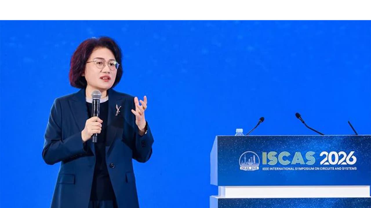
Huawei is pioneering a new 'Tau Scaling' principle for chip design, moving beyond Moore's Law. It focuses on reducing signal transmission time rather than just shrinking transistors, using innovations like LogicFolding for its upcoming Kirin chips.
China's electronics giant Huawei is using a new principle for its chip designing framework that focuses more on cutting transmission time than shrinking transistors. The company plans to use innovative technologies like LogicFolding based on this principle to continuously compress signal propagation delay and improve transistor density.
From Moore's Law to Tau Scaling
The current chip design framework rests on Moore's law which dates back decades when Intel co-founder Gordon Moore posited in 1965 that the number of transistors on a microchip will double every two years. The Tau Scaling principle could be a revolutionary step in the future of chip designing as it shifts focus from geometric scaling to time scaling.
The principle that governs modern advanced chips is to shrink the size of transistors to fit onto a microchip. But this mechanism may have a handicap. It may not be easy to shrink them beyond a point. This is where time scaling becomes useful as it makes cutting signal transmission time the underlying principle of future chip designs.
The innovative core technologies like LogicFolding, which Huawei will use for its Kirin chips scheduled to launch in Fall 2026, will work on the Tau Scaling principle in order to drive up performance, energy efficiency, and transistor density. "With the t Scaling Law, we look forward to working closely with scientists, engineers, and industry partners around the world to drive the sustainable development of the semiconductor and electronics industries," Huawei's semiconductor chief He Tingbo noted.
Bypassing Sanctions and Future Goals
Huawei's new chip design breakthrough will help the chip maker to sidestep the US sanctions that restrict access to advanced lithography machines from ASML. By 2031, Huawei is aiming for high-end chips based on the t Scaling Law that are expected to feature a transistor density that is equivalent to 14 A (1.4 nm) processes.
Industry Perspective and Potential Hurdles
"This is a breakthrough for Huawei, but it's not a threat for TSMC," Reuters quoted Nvidia CEO Jensen Huang, who was in Taipei on Thursday. "TSMC has been using die stacking and 3D packaging for how long now? Almost 10 years. And so TSMC's technology is very advanced," he added. A Reuters report mentioned Bernstein analysts cautioning in a note that while stacking multiple chip layers boosts transistor density, there's risk of increasing power density and overheating chips. (ANI)
(Except for the headline, this story has not been edited by Asianet Newsable English staff and is published from a syndicated feed.)