India Boosts Electronics Manufacturing With 12 New Projects Approved
Synopsis
India has approved 12 new electronics projects under the ECMS worth Rs 7,503 crore, aiming to boost domestic manufacturing, create thousands of jobs, and strengthen the upstream electronics and battery materials ecosystem.
Boosting Domestic Electronics Manufacturing
India is stepping up efforts to build domestic capabilities in critical electronics materials and manufacturing equipment, with the government approving 12 additional projects worth Rs 7,503 crore under the Electronics Component Manufacturing Scheme (ECMS), marking a shift towards strengthening the upstream segments of the electronics value chain. Electronics and Information Technology Secretary S Krishnan said the latest approvals would help establish domestic manufacturing capabilities in materials and capital goods, including the country's first commercial cathode material manufacturing unit.
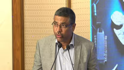
Speaking at the launch of the Semicon 2.0 web application portal and announcement of approved ECMS applicants, Krishnan said the projects are expected to generate production worth more than Rs 39,000 crore and create over 7,000 jobs. He highlighted that the government's approach was not limited to manufacturing components for specific end-use industries, but aimed at creating a broader materials ecosystem that could support multiple sectors, including electronics and batteries.
Expansion of the ECMS Scheme
The latest approvals include projects under Segment D of ECMS, which focuses on materials required for electronics manufacturing, along with three projects related to capital goods. Krishnan said the government was also examining further applications and possible modifications to the scheme to accommodate industry requirements, as applications have already crossed the enhanced budgetary allocation of Rs 40,000 crore.
So far, 118 applications covering 34 products across 16 states have been approved under ECMS. Against the original investment target of Rs 59,350 crore, approved investments have reached Rs 77,051 crore, while projected production has increased from Rs 4.56 lakh crore to Rs 5.73 lakh crore. The approved projects are expected to generate 81,755 jobs, against the original target of 91,600.
Launch of Semicon 2.0 Initiative
Separately, the Ministry launched the application portal for three pillars of the Semicon 2.0 programme, which carries a total outlay of Rs 1,27,500 crore. These cover semiconductor equipment and materials, fabrication facilities, and packaging, with advanced packaging identified as a priority area. Krishnan said the new application window would allow industry players to submit proposals across these segments, building on the semiconductor projects approved under the first phase of the programme.
Stay updated with all the latest Business NewsShare Market NewsIPOsGold PriceDA Hike8th Pay CommissionAsianet News Official App