IBM debuts world's first sub-1 nanometer chip with 100B transistors
Synopsis
IBM unveiled the world's first sub-1 nanometer chip, a 0.7nm node packing 100 billion transistors. The new 3D nanostack architecture offers twice the density of 2nm chips and boosts performance by 50% for AI and cloud applications.
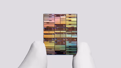
IBM debuted the world's first sub-1 nanometer chip technology, introducing a transistor architecture at the 0.7 nanometer, or 7 angstrom node. IBM noted that this new chip packs nearly 100 billion transistors into a space the size of a fingernail. This represents nearly twice the transistor density of the company's 2-nanometer chip, which was introduced in 2021.
Microchips play crucial roles in computing, home appliances, communication devices, transportation networks, and critical infrastructure systems. IBM projects a path to commercial production for the sub-1 nanometer technology within the next five years. The development relies on structural and material modifications, specifically a three-dimensional nanostack architecture.
Enhanced Performance and Energy Efficiency
As per the company, published technical reports project that the design offers up to a 50 per cent increase in performance, or a 70 per cent reduction in energy consumption compared to existing 2-nanometer nodes. This capability is expected to support generative artificial intelligence, cloud infrastructure, and next-generation electronic devices.
Reinventing Chip Architecture
"IBM's latest chip breakthrough marks a landmark moment in computing, pushing technology beyond the nanometer era to the scale of atoms," said Jay Gambetta, Director of IBM Research and IBM Fellow. He added, "With our new nanostack architecture, we're not just making smaller transistors, we're reinventing how chips are built to deliver dramatically more power and energy efficiency."
The design vertically stacks and staggers transistors through 3D sequential integration, allowing different material combinations within each layer to optimize power and performance independently.
Technical Validation
According to data from IBM, researchers validated the architecture through ultra-thin dielectric bonding in complementary metal-oxide-semiconductor (CMOS) integration, demonstrating dual-channel engineering and functional CMOS inverter operation. Research presented at the VLSI 2026 conference also showed that the architecture provides a 40 per cent scaling reduction in static random-access memory (SRAM), which aids high-bandwidth data demands for artificial intelligence workloads.
Future of Computing and Scaling Roadmap
Gambetta stated, "This industry-first innovation continues IBM's legacy of leading in next-generation technologies and sets the foundation for the next era of computing."
The 0.7 nanometer technology marks the first time logic scaling extends below the 1 nanometer threshold into angstrom-level dimensions. While modern node names represent generations of manufacturing technology rather than exact physical measurements, the organization projects that the architecture provides a semiconductor roadmap for at least a decade of future scaling.
Collaborative Development
Research and development for this project took place at a facility in Albany, New York, in collaboration with partners including Lam Research Corp., Tokyo Electron, and SCREEN Semiconductor Solutions, Ltd. The facility is scheduled to integrate a High Numerical Aperture Extreme Ultraviolet lithography tool developed by ASML to print the precise circuits. (ANI)
(Except for the headline, this story has not been edited by Asianet Newsable English staff and is published from a syndicated feed.)Stay updated with all the latest Business News, including market trends, Share Market News, stock updates, taxation, IPOs, banking, finance, real estate, savings, and investments. Track daily Gold Price changes, updates on DA Hike, and the latest developments on the 8th Pay Commission. Get in-depth analysis, expert opinions, and real-time updates to make informed financial decisions. Download the Asianet News Official App from the Android Play Store and iPhone App Store to stay ahead in business.